Institut für Angewandte Physik

Research

Research summary:

We explore the cornupia of new physics that can be accessed with the latest developments in the materials sciences, in particular low-dimensional (two-dimensional) new materials, in combination with cutting edge aberration-corrected transmission electron microscopy. We employ cutting edge microscopic analysis and also develop new methods to study the sometimes highly radiation sensitive atomic configurations. Moreover, we use microscopic tools to manipulate materials at the atomic level.

Graphene, a single layer of carbon atoms, was the first 2D material and generated an enormeous interest for basic science and potential applications. It features an extraordinary electronic structure, a record mechanical stability, highest current carrying capabilities and thermal conductivity, the largest surface area per volume as well as a relatively inert surface. Freely suspended mono-layer graphene is the thinnest possible membrane that is conceivable with currently known materials. Yet, it is remarkably stable under high-energy electron irradiation, and thus opens unprecedented opportunities also for electron microscopic studies. Among other things, it may serve to encapsulate other, more radiation sensitive objects such as layers of molecules. Besides graphene, there exists now a whole zoo of 2D materials with a wide variety of electronic, mechanical or chemical properties which can be further tailored by defects, dopants or functionalization.

The remarkable developments in electron microscopy over the past few years, in particular the correction of lens aberrations⁠ and reduction of electron energies, have enabled the direct imaging of the exact atomic structure even in materials made of light elements and of low dimensionality. We can now study these materials with unprecedented precision and follow dynamic processes in in-situ experiments. Exploring new avenues in this direction is one part of our research focus.

The image shows an aberration-corred scanning transmission electron microscope (STEM) image of single layer graphene, in which individual carbon atoms are resolved (some of the carbon atoms are indicated as illustration). The dark area on the bottom left is a hole in the graphene sheet, formed by electron irradiation.


Research examples (includes works from previous affiliations of J. Meyer)

Aligned Stacking of Nanopatterned 2D Materials for High-Resolution 3D Device Fabrication

Structuring matter on the smallest dimensions is a key capability for many areas of technology. Here, we combine spatially controlled modifications of 2D materials, using focused electron irradiation or electron beam induced etching, with the layer-by-layer assembly of van der Waals heterostructures. In particular, we have found a method that enables a stacking of the pre-structured layers with very accurate lateral alignment. In this way, arbitrary 3-D structures can be formed, akin to the layer-by-layer assembly in many 3D printing procedures. However, with the individual layers being only one atom thick, the layer structuring  in the scanning transmission electron microscope reaching atomic dimensions, and layer alignment accuracy currently in the few-nanometer range, this fabrication method is not far from atomic-resolution 3D printing, and could arguably get there with further improvement. Moreover, as the material in each layer can be chosen from the vast zoo of 2D materials, it should become possible to directly fabricate functional devices, which will be the subject of further research.

The research was carried out at the University of Tübingen and at the Natural and Medical Sciences Institute by J. Haas, F. Ulrich, C. Hofer, K. Braun, and J. C. Meyer and at Hunan University, China, by X. Wang. The publication in ACS Nano can be found at https://doi.org/10.1021/acsnano.1c09122

Atomic-resolution microscopy reveals oxygen with three carbon neighbors

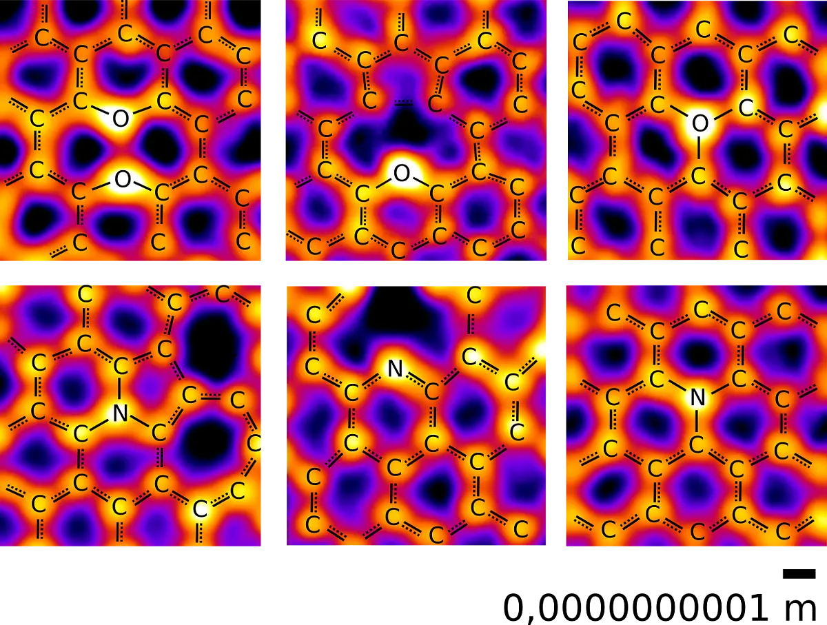
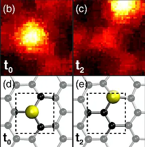
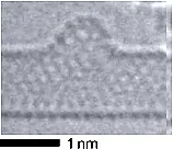
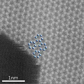
Organic chemistry textbooks say that carbon forms up to four bonds, nitrogen up to three, and oxygen only one or two covalent bonds, corresponding to the number of unpaired electrons in the outermost shell. We have studied the bonding of a large number of nitrogen and oxygen atoms incorporated into a carbon matrix (defective graphene) using scanning transmission electron microscopy.

Remarkably, we found that some of the oxygen atoms had three carbon neighbors, among a large variety of other configurations. So far, oxygen with three bonds was only known in a highly charged state, referred to as oxonium, which is difficult to stabilize in extended compounds. Here, however, the oxygen atoms were contained in an extended carbon matrix and showed a remarkable stability by surviving the high dose of high-energy electron irradiation required for their imaging.

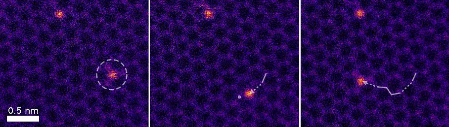
The image shows a variety of bonding configurations oxygen and nitrogen atoms in the carbon matrix. The study further revealed that oxygen quite frequently bonds in a “pair” configuration in which two oxygen atoms occupy neighboring sites in the graphene lattice, while not being close enough to form a bond. Individual oxygen and nitrogen atoms tend to occupy edges of small holes, bonded to only two carbon neighbors. While the textbook concept of bonding for carbon, nitrogen and oxygen is thus mostly confirmed, also for the extended material, it appears that these common elements can still yield surprises.

The work was carried out at the University of Vienna and the University of Tübingen by C. Hofer, V. Skakalova, T. Görlich, M. Tripathi, A. Mittelberger, C. Mangler, M. Monazam, T. Susi, J. Kotakoski and J. C. Meyer. The publication in Nature communications can be found at https://www.nature.com/articles/s41467-019-12537-3.


The 3D structure of defects in graphene

We developed a new route to measure the 3D structure of graphene and its defects from only two atomically resolved images recorded with slightly different sample tilt. An atomistic model is optimized until simulated images agree with the experimental one. In this way, we have obtained (shown from top to bottom in the image) the 3D structure of a grain boundary in graphene, of a cluster of four silicon atoms in graphene, and of a graphene sheet that was distorted by a physisorbed carbon nanotube.

The work was carried out by C. Hofer, K. Mustonen, M. Monazam, V. Skakalova, A. Mittelberger, G. Argentero, C. Mangler, K. Elibol, T. Susi, J. Kotakoski and J. Meyer at the University of Vienna and by A. Hussain, P. Laiho, H. Jiang and E. Kauppinen at Aalto University, Finland. The three publications are (1) https://doi.org/10.1088/2053-1583/aaded7  (2) https://doi.org/10.1063/1.5063449  (3) https://doi.org/10.1021/acsnano.8b04050 .

Graphene-Fullerene sandwiches: The nano-scale petri dish

We demonstrated the first direct images of a suspended 0D/2D heterostructure that incorporates C60 molecules between two graphene layers in a buckyball sandwich structure. We find clean and ordered C60 islands with thicknesses down to one molecule, shielded by the graphene layers from the microscope vacuum and partially protected from radiation damage during scanning transmission electron microscopy imaging. The sandwich structure serves as a 2D nanoscale reaction chamber, allowing the analysis of the structure of the molecules and their dynamics at atomic resolution. Among other things, we could quantify the diffusion of the molecules and observe the transition from rotating to fixed molecules as they merge into larger clusters.

The work was carried out at the University of Vienna by R. Mirzayev, K. Mustonen, M. Monazam, A. Mittelberger, T. J. Pennycook, C. Mangler, T. Susi, J. Kotakoski and J. C. Meyer and the paper can be found at https://advances.sciencemag.org/content/3/6/e1700176

Insights into radiation damage by atomic-resolution imaging of Chlorinated copper phtalocyanine on graphene

We imaged a single layer of chorinated copper phtalocyanine (ClCuPc) on graphene. These molecules are destroyed already at very low doses of electron irradiation, which makes it impossible to obtain atomic resolution images in the usual way.  However, by configuration averaging it was possible to reveal the original structure of the molecule. At higher doses, under direct observation, the molecules formed disordered, cross-linked networks where the heavy copper atom was still present. The study provided unique insights into the mechanism of radiation damage, e.g. the dissociation of the chlorine atoms at low doses while the remainder of the molecule was relatively radiation hard.

The research was carried out at the University of Vienna by A. Mittelberger, C. Kramberger, and J. C. Meyer. The publication can be found here: https://www.nature.com/articles/s41598-018-23077-z

Beam-driven Silicon-Carbon Bond Inversions for controlled relocation of Silicon impurities in Graphene

In this study we demonstrated that 60-keV electron irradiation drives the displacement of threefold-coordinated Si dopants in graphene by one lattice site at a time. First principles simulations reveal that each step is caused by an electron impact on a C atom next to the dopant.  The results indicate a route for a nondestructive and atomically precise structural relocation of the impurity.

This work was carried out in a collaboration by D. Kepaptsoglou and Q. Ramasse from the SuperSTEM Laboratory (UK), R. Zan and U. Bangert from the University of Manchester (UK), T. C. Lovejoy and O. L. Krivanek from Nion Co. (US), and T. Susi, J. Kotakoski, C. Mangler, P. Ayala, J. C. Meyer from the University of Vienna (AT). The Physical Review Letters paper can be found at https://journals.aps.org/prl/abstract/10.1103/PhysRevLett.113.115501.


Later, the controlled displacement of a silicon impurity by one atomic distance in each step was demonstrated experimentally. It was first shown in the article “ Manipulating low-dimensional materials down to the level of single atoms with electron irradiation”, which is partly a review and partly showing new results, and can be found at https://doi.org/10.1016/j.ultramic.2017.03.005.

Imaging the atomic-level random walk of a point defect in graphene

The diffusion of defects in solids is behind many microstructural changes in solids. Here, we stimulated and followed the migration of a divacancy through the graphene lattice using a scanning transmission electron microscope operated at 60 kV. The beam-activated process happens on a timescale that allows us to capture a significant part of the structural transformations and trajectory of the defect.  The low voltage combined with ultra-high vacuum conditions ensures that the defect remains stable over long image sequences, which allowed us to directly follow the diffusion of a point defect in a crystalline material.

This work was carried out at the University of Vienna by J. Kotakoski, C. Mangler and J. C. Meyer and our publication in Nature communications can be found at

http://www.nature.com/ncomms/2014/140529/ncomms4991/full/ncomms4991.html

A new route to circumvent radiation damage

We introduced a new approach to circumvent the radiation damage problem by a statistical treatment of large, noisy, low-dose data sets of non-periodic configurations. On the basis of simulated data, we demonstrated that high-resolution images can be reconstructed from very low dose exposures of repeatedly occurring structures (e.g. defects, functional groups, small molecules). The only prerequisite is that there is a finite set of different configurations that appear repeatedly on a large area, imaged at very low dose where no damage is expected to occur.

The idea and proof of concept was published in Ultramicroscopy and is accessible at www.sciencedirect.com/science/article/pii/S0304399113003100 . Experimental realizaton was shown later, the article can be found at doi.org/10.1002/pssb.201700176 . The research was carried out at the University of Vienna by C. Kramberger, A. Mittelberger, C. Hofer, J. Kotakoski, C. Mangler and J. C. Meyer.

A journey from Order to Disorder

ne of the most interesting questions in solid state theory is the structure of glass, which has eluded researchers since the early 1900's. Here, we presented a direct, atomic-level structural analysis during a crystal-to-glass transformation, including all intermediate stages. We introduced disorder on a 2D crystal, graphene, gradually, utilizing the electron beam of a transmission electron microscope, which allows us to capture the atomic structure at each step. We identified three regimes of the disordered system, namely the crystal with point defects, individual crystallites separated by a vitreous network, and a fully vitreous random network.

Our paper in Scientific Reports by F. Eder, J. Kotakoski, U. Kaiser and J. C. Meyer can be found at http://www.nature.com/articles/srep04060.

Reshaping graphene via dual-probe microscopy

We showed that we can access the same point on both surfaces of a few-layer graphene membrane simultaneously, using a novel type of dual-probe scanning tunneling microscopy (STM) setup. With the two STM probes approaching the membrane from opposing sides, we were for the first time able to directly measure the deformations induced by one STM probe on a free-standing membrane with an independent second probe. We revealed different regimes of stability of few-layer graphene, and showed how the STM probes can be used as tools to shape the membrane in a controlled manner. Our work opens new avenues for the study of mechanical and electronic properties of two-dimensional materials.

See our publication in Nano letters at http://pubs.acs.org/doi/abs/10.1021/nl3042799. The research was carried out at the University of Vienna by F. Eder, J. Kotakoski, K. Holzweber, C. Mangler, V. Skakalova, and J. C. Meyer.

Transformations of carbon on graphene under extreme heat

We showed a reorganization of carbon adsorbates by in situ atomic-resolution transmission electron microscopy (TEM) performed on specimens at extreme temperatures. By using graphene sheets at the same time as ultra-transparent TEM substrate and as in-situ heater, we can create a new nanocrystalline graphene layer on top of the existing membrane. The new layer displays domain sizes of 1-3 nanometer and open edges with predominantly armchair configuration.

See our Nano Letters article at  http://pubs.acs.org/doi/abs/10.1021/nl203224z. This research was carried out at the University of Ulm, Germany, by B. Westenfelder, J. C. Meyer, J. Biskupek, S. Kurasch, F. Scholz, C. E. Krill, and U. Kaiser.

Reactions of the inner surface of carbon nanotubes imaged at the atomic scale

In this study, we showed that in the presence of catalytically active atoms of rhenium inserted into nanotubes, the nanotube sidewall can be engaged in chemical reactions from the inside.

See the Nature Chemistry article at http://dx.doi.org/10.1038/NCHEM.1115. The research was carried out at the University of Nottingham, UK, and at the University of Ulm, Germany, by T. W. Chamberlain, J. C. Meyer,  J. Biskupek, J. Leschner, A Santana, N. A. Besley, E. Bichoutskaia,  U. Kaiser, and A. N. Khlobystov.

Analysis of charge transfer in nitrogen-doped graphene and hexagonal boron nitride

For the first time, we demonstrated that the charge density redistribution in chemical bonds can be analyzed from high accuracy high-resolution TEM measurements.  This opens a new route to analyze the electronic configuration, and it is particularly suited for non-crystalline configurations such as point defects where an analysis by reciprocal space methods is not possible.

At the same time, our study shows for the first time a direct visualization of individual nitrogen dopants in mono-layer graphene and demonstrates a change in the electronic configuration of the nearest-neighbor carbon atom next to the dopant.

See the Nature Materials article at http://dx.doi.org/10.1038/nmat2941. The research was carried out at the University of Ulm, Germany, and at the Max Planck Institute for solid state research, Stuttgart, Germany, by J. C. Meyer, S. Kurasch, H.-J. Park, V. Skakalova, D. Künzel, A. Groß, A. Chuvilin, G. Algara-Siller, S. Roth, T. Iwasaki, U. Starke, J. Smet and U. Kaiser.

Creating carbon atomic chains from graphene

We formed single-atomic carbon chains by thinning a graphene constriction under the electron beam. The chains formed efficiently by self-organization during continuous removal of atoms from a graphene bridge. These new molecular structures may provide a novel element for all-carbon electronics.

See our article in the New Journal of Physics at http://dx.doi.org/10.1088/1367-2630/11/8/083019. This research was carried out at the University of Ulm by A. Chuvilin, J. C. Meyer, G. Algara-Siller, and U. Kaiser. (a similar discovery was made at about the same time by K. Suenaga and colleagues from AIST, Tsukuba, Japan, their article can be found here: http://link.aps.org/doi/10.1103/PhysRevLett.102.205501.)


The graphene edge

The boundary of a 2-D material is a 1-D line of atoms. The 2009 paper in Science showed the first aberration-corrected high resolution images and videos of the open edge configurations in free-standing graphene and their dynamic rearrangement.

See the article and supplementary videos at http://dx.doi.org/10.1126/science.1166999. This work was carried out at the University of California at Berkeley and at the Lawrence Berkeley National Laboratory, Berkeley, USA by C. O. Girit, J. C. Meyer, R. Erni, M. D. Rossell, C. Kisielowski, L. Yang, C.-H. Park, M. F. Crommie, M. L. Cohen, S. G. Louie and A. Zettl.

Ultra-high resolution pattern definition on graphene

Using electron-beam induced deposition (EBID, also known as contamination lithography) we wrote smallest structures with a resolution down to 2.5nm (half-pitch) on top of a graphene membrane. Such patterns may provide a route to create nanometer-scale doping patterns, diffraction gratings, or etch masks in this novel electronic material.

The article in Applied Physics Letters can be found here: http://dx.doi.org/10.1063/1.2901147. The research was carried out at the University of California at Berkeley and at the Lawrence Berkeley National Laboratory, Berkeley, USA by J. C. Meyer, C. O. Girit, M. F. Crommie and A. Zettl.

The structure of suspended graphene sheets

Our studies by transmission electron microscopy revealed that suspended graphene sheets are not perfectly flat: they exhibit intrinsic microscopic roughening such that the surface normal varies by several degrees and out-of-plane deformations reach 1 nm.

Our letter to Nature can be found at http://dx.doi.org/10.1038/nature05545. The research was carried out at the Max Planck Institute for solid state research, Stuttgart, Germany, the University of Manchester, UK, and the University of Nijmegen, Netherlands, by J. C. Meyer, A. K. Geim, M. I. Katsnelson, K. S. Novoselov, T. J. Booth and S. Roth.

The single-molecule torsional pendulum

A single-walled carbon nanotube served as a molecular-scale torsional spring and as mechanical support in this nano-electromechanical device (the scale bar on the image sequence to the right is ca. 500 nanometer.). We were able to determine the handedness of the carbon nanotube and observed the thermally induced vibrations in direct images. Devices of this type might serve as extremely sensitive nano-scale sensors.

Our report in Science can be found at http://dx.doi.org/10.1126/science.1115067. This work was carried out at the Max Planck Institute for solid state research, Stuttgart, Germany, and the Universite de Montpellier, France, by J. C. Meyer, M. Paillet, and S. Roth.