Single electron transistors in silicon
Due to the steady downscaling of CMOS (complementary metal oxide semiconductor) devices, the transport properties of the transistors are increasingly dominated by so far unwanted effects, like charging effects and quantum mechanical effects. Single electron transistors (SETs), whose functionality is determined by the Coulomb blockade, offer a possible solution to this problem. SETs are also extremely sensitive to electrical charges. An SET can sense the charge changes by a single electron. Detection of nanoscale displacement is also possible.
For the EU project AFSID CMOS-compatible SETs on 8-inch wafers have been fabricated by CEA-LETI [1]. These consist of silicon nanowires and polysilicon topgates. Transport measurements on these devices show outstanding Coulomb diamonds with charging energies up to some 10 meV, which bring room temperature operation within reach. Double and multi dot structures, which are key structures for quantum circuits, have also been realized.
a) Coulomb diamond and excited states,
b) signature of a dopant, c) honeycomb pattern of a double dot
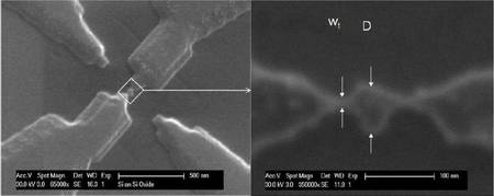
For SETs fabricated in Tübingen, the tunnel barriers are realized through geometrical constrictions of the silicon nanowire. For this approach the SETs are fabricated on SOI (silicon on insulator) wafers by means of techniques such as electron beam lithography and reactive ion etching. Afterwards metal contacts are evaporated and contacted with wire bonding. That way quantum dots with diameters of 40 nm and tunnel barriers of 10 nm width have been realized [2].

SEM image of an SET
(left: overview, right: magnified view of the critical area)
[1] M. Pierre, X. Jehl, R. Wacquez, M. Vinet, M. Sanquer, M. Belli, E. Prati, M. Fanciulli, J. Verduijn, G.C. Tettamanzi, G.P. Lansbergen, S. Rogge, M. Ruoff, M. Fleischer, D.A. Wharam, D.P. Kern. Sample variability and time stability in scaled silicon nanowires. Proc. 10th Int. Conf. Ultimate Integration of Silicon ULIS, 249 (2009).
[2] W. Daves, M. Ruoff, M. Fleischer, D.A. Wharam, D.P. Kern. Hydrogen silsesquioxane electron beam lithography for ultra-small single electron transistors in silicon on insulator. Microelectron. Eng. 87, 1643 (2010).
[3] X. Jehl, B. Roche, M. Sanquer, B. Voisin, R. Wacquez, V. Deshpande, B. Previtali, M. Vinet, J. Verduijn, G.C. Tettamanzi, S. Rogge, D. Kotekar-Patil, M. Ruoff, D.P. Kern, D.A. Wharam, M. Belli, E. Prati, M. Fanciulli. Mass production of silicon MOS-SETs: Can we live with nano-devices' variability? Proc. Comp. Sci. 7, 266 (2011).
