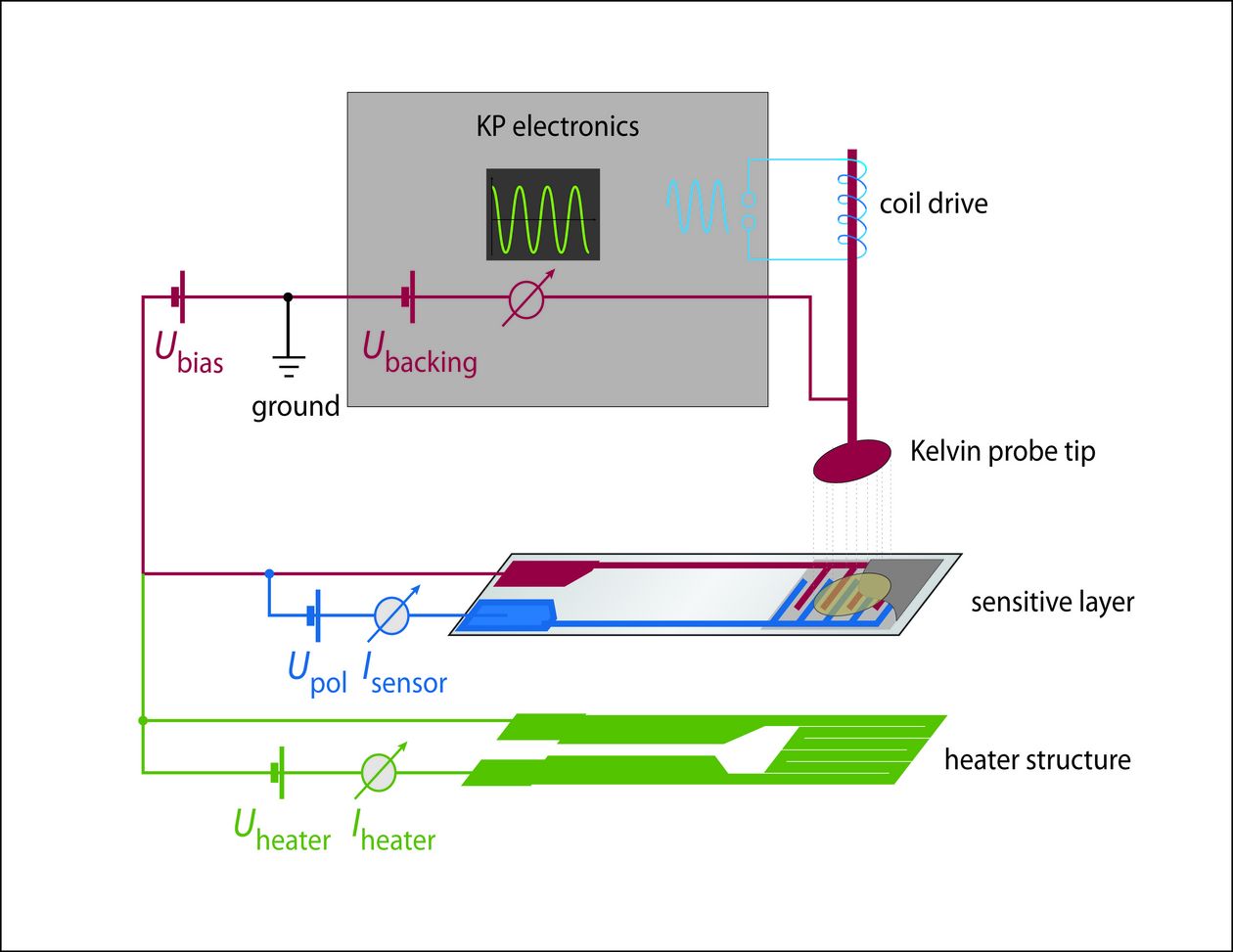
The work function of a semiconductor is the least amount of energy required to remove an electron from the Fermi level to a point far enough not to feel any influence from the material, with zero kinetic energy. As the electron has to move through the surface region, the work function is extremely sensitive towards changes at the surface caused by gaseous interaction. Simultaneous work function and resistance changes measurements in operando conditions for sensors (in air, in the presence of humidity and target gases, with heated sensors, etc) are performed in our lab by using the Kelvin Probe technique. The latter is a non-contact, non-destructive method that uses a vibrating reference electrode to measure the changes of the contact potential difference (CPD) between the sample and the electrode. Therefore, the Kelvin Probe technique only allows to measure changes of the work function determined by changes in the composition of the ambient atmosphere, not absolute values; variations in the CPD induced by the changes in the test gas atmosphere represent layer’s relative work function variations. By simultaneously measuring the changes in the layer’s resistance one gains insight about the conduction mechanism in the sensing layer and the way in which the surface charge transfer impacts on that one. Besides that, it is possible to de-convolute the different contributions to the work function, namely the band bending and the electron affinity of the surface.
