Center for Light-Matter Interaction, Sensors & Analytics (LISA+)

Topography and Film Thickness Measurement

AFM   |   Profilometer   |   Ellipsometer

AFM - Atomic Force Microscope

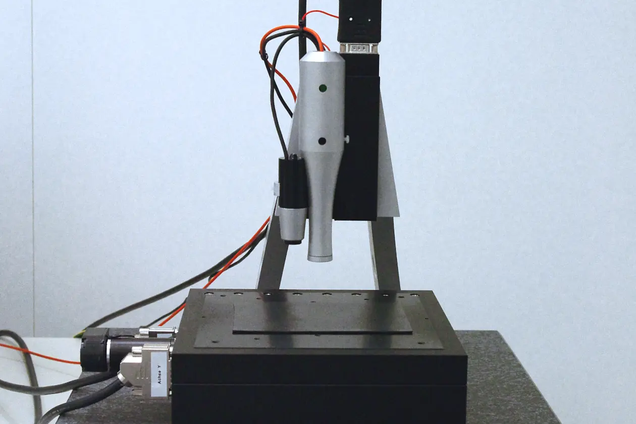
With the atomic force microscope (AFM), a cantilever of approx. 100 µm length with a fine tip (typically approx. 10 µm high, 10 nm radius) is brought into contact with the surface and rastered over the scanning area. The bending of the cantilever is detected by a laser detector system. A control loop detects the deflection and adjusts the height of the cantilever during the scan to keep the preset deflection constant. The height change is recorded for each scan pixel, creating a 3D image of the surface.

Other operating modes of an AFM the cantilever is driven close to its resonance frequency. At this frequency, the amplitude of the oscillation reacts extremely sensitive to changes in the interacting forces, which in turn depend very strongly on the distance between the tip and the surface. The measurement is now carried out by readjusting the position of the cantilever to keep the amplitude constant. Measurement can be carried out either completely contactless or by continuously placing the tip on the surface.

Apart from the imaging operating modes, force curves can also be recorded with an AFM to determine, for example, the elasticity modulus of a substrate or to determine the adhesion forces of molecules, biological cells or bacteria. In addition, friction forces can be investigated. With the use of appropriate cantilevers, magnetic or electrical fields can also be mapped.

Veeco (DI) NanoScope

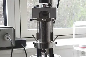
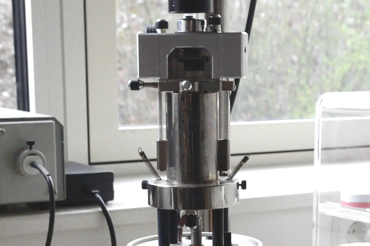
The NanoScope is equipped with a specimen camera, which makes it very easy to align the substrate under the cantilever. The standard scanner offers a scanning range of 150 x 150 x 5 µm. Alternatively, a high-precision scanner can be installed that limits the scanning range to 0.4 x 0.4 x 0.4 x 0.4 µm. A wet cell and a scanning tunneling scanner are also available.


Tactile Profilometer

A tactile profilometer scans a surface with a diamond tip, the stylus. Elevations and depressions of the surface deflect the stylus. This deflection is registered by means of a Linear Variable Differential Transformer (LVDT) and converted into an image of the surface. A profilometer allows standard line scanning to measure step heights or surface roughness, 3D mapping to display and analyze the substrate surface in three dimensions, and stress calculation in deposited layers by measuring the bending of a substrate surface.

Bruker Dektak XT-A

Our Dektak XT-A has an automated 150 x 150 mm stage. The measuring head travels over an optically flat glass block with a travel of 55 mm. Scanning lengths of up to 200 mm are possible by automated stitching. The maximum sample height is 50 mm.

Step heights can be measured in a range from < 10 nm to max. 1 mm with a repeatability of < 0.4 nm (at 1 µm step height).

The standard stylus has a tip radius of 12.5 µm. For higher requirements a stylus with a radius of 2 µm is available.

All users of LISA+ have access to the Vision64 software with a wide range of display options and analysis functions. The data can also be exported for other programs in ASCII format.


Optical Profilometer

With an optical profilometer, the surface is not measured mechanically but by means of a focused light beam. The light passes through an optical lens in the measuring head with a strong chromatic aberration so that the focal length in the blue to red range of the spectrum varies by more than 300 µm. If a substrate is scanned with the measuring head, the focus of different wavelengths is on surface elevations and depressions. The reflected light is collected via the same lens and analysed with a spectrometer. Since the focussed area of the spectrum contributes the most to the intensity of the measurement signal, the distance of the surface to the measuring head can be calculated.

FRT MicroProf 100

The FRT MicroProf 100 enables fast and non-destructive surface analysis. The travel distance of the stage is 100 x 100 mm and allows a max. measuring speed of 100 mm/sec. The maximum sample height is 50 mm. The height measuring range is max. 300 µm with a resolution of 10 nm.


Monochromatic Ellipsometer

In ellipsometry, the polarization change of a reflected light beam on a substrate is analyzed to determine the dielectric properties of thin films or their layer thickness. Once the thin films have been sufficiently precise defined, further conclusions can be drawn from the dielectric properties of the material regarding composition, crystal structure, anisotropy, conductivity, doping or roughness.

For the analysis, the incident light is initially polarized linearly and directed onto the substrate. Polarization is usually adjusted at an angle of 45° to the plane of incidence, so that the electromagnetic field of the incident beam can be divided equally into a parallel and a vertical component. The behaviour of these components in the reflection on a thin film or layer system can be described by the Fresnel formulas.

An analyzer detects the amplitude ratio and phase shift of the vertical and parallel components in the reflected beam. In addition to these measured values, a model system is also required which is created from the known parameters, e. g. layer thicknesses of the thin film or the layer system. The analysis software now adapts the parameters still unknown from the model in Fresnel's formulas until the experimental data are reproduced with the smallest possible error.

DRE Enhanced EL X-02C

The EL X-02C is a monochromatic ellipsometer with a wavelength of 632.8 nm (HeNe-Laser) and an outstanding sensitivity of the Enhanced model with 0.001 nm - 0.01 nm for SiO2 on silicon. The angle of incidence can be adjusted manually from 45° - 90° in 5° steps. Coating thicknesses can typically be determined from < 1Å to < 1 mm, but metallic layers are usually only suitable for measurements in ellipsometers up to approx. 100 nm.